


解决方案
PhotoCAD应用—实现任意光子晶体建模
光子晶体是一种由周期性结构构成的材料,能够建立光子带隙,从而实现光子的操纵。为了让用户更方便地使用PhotoCAD搭建光子晶体链路模型,我们提供了本教程。通过简化输入参数,用户只需根据脚本输入光子晶体的行列数(周期数)、间隙以及基础单元模型等参数,即可快速实现光子晶体的建模。这样的设计让用户能够更轻松地理解和操作光子晶体,为相关领域的研究和应用提供了便利。
1.光子晶体简介
光子晶体是一种具有周期性结构的人工材料,能够控制光传播的方向和速度。这种材料具有许多独特的光学特性,如光子带隙和光子局域化等。光子带隙是指光子晶体能够阻止特定频率的光通过,而光子局域化则是光子晶体能够将光场局域在某些特定区域。这些特性使得光子晶体在光量子计算机、传感器、光学成像等领域都有广泛的应用前景。
2.光子晶体结构的版图实现
光子晶体为周期结构,基本单元也从传统的单一规则结构演变成多个基本结构组合的结构到没有规律的拓扑结构。教程提供的代码从底层出发,支持用户自定义周期结构,在用户定义的周期结构的基础上通过几个简单参数即可实现任意光子晶体链路的搭建。
import math
from fnpcell import all as fp
from typing_extensions import Tuple, List, cast
from gpdk import all as pdk
from gpdk.technology import get_technology
from gpdk.technology.wg.types import CoreCladdingWaveguideType
import numpy as np


class PhC(fp.PCell):
    """
    Attributes:
        PhC_row
        PhC_column
        PhC_width
        PhC_length
        PhC_gap
        waveguide_type

    Examples:
    PhC = PhC(PhC_row=6, PhC_column=12, PhC_rowgap=120, PhC_columngap=120, PhC_gap=200)
    """

    ## init parameters
    PhC_row: int = fp.PositiveIntParam(default=8)
    PhC_column: int = fp.PositiveIntParam(default=10)

    PhC_rowgap: float = fp.PositiveFloatParam(default=120)
    PhC_columngap: float = fp.PositiveFloatParam(default=120)
    PhC_gap: float = fp.PositiveFloatParam(default=200)

    wavegide_type: CoreCladdingWaveguideType = fp.WaveguideTypeParam(
        type=CoreCladdingWaveguideType, default=get_technology().WG.FWG.C.WIRE
    )

    def build(self):
        ## initial
        insts, elems, ports = super().build()

        ## define module
        ## double circle
        para_main = 50
        para_aux = 30
        module_main = fp.el.Circle(
            radius=para_main,
            layer=self.wavegide_type.core_layer,
        )
        module_aux = fp.el.Circle(
            radius=para_aux,
            layer=self.wavegide_type.core_layer,
        )
        module = module_main.translated(0, 0) | module_aux.translated(80, 20)

        # ## double triangular
        # para_main = 50*2#*np.sqrt(3)/2
        # para_aux = 30*2#*np.sqrt(3)/2
        # ## state1
        # # module_main = fp.el.Polygon(
        # #     raw_shape=[(-para_main/2,0),(para_main/2,0),(0,para_main*2/np.sqrt(3))],
        # #     layer=self.wavegide_type.core_layer
        # # )
        # # module_aux = fp.el.Polygon(
        # #     raw_shape=[(-para_aux/2,0),(para_aux/2,0),(0,para_aux*2/np.sqrt(3))],
        # #     layer=self.wavegide_type.core_layer
        # # )
        # # module  = module_main.translated(0,0) | module_aux.translated(80,(para_main-para_aux)*2/np.sqrt(3))
        # ## state2
        # module_main = fp.el.Polygon(
        #     raw_shape=[(-para_main/2,0),(para_main/2,0),(0,-para_main*2/np.sqrt(3))],
        #     layer=self.wavegide_type.core_layer
        # )
        # module_aux = fp.el.Polygon(
        #     raw_shape=[(-para_aux/2,0),(para_aux/2,0),(0,-para_aux*2/np.sqrt(3))],
        #     layer=self.wavegide_type.core_layer
        # )
        # module  = module_main.translated(0,0) | module_aux.translated(80,-(para_main-para_aux)*2/np.sqrt(3))

        ## trans parameters
        PhC_width = (
            self.PhC_column * (para_main + self.PhC_columngap)
            + self.PhC_columngap
            - 0.5 * para_main
        )
        PhC_height = (
            2 * self.PhC_row * (self.PhC_rowgap + para_main)
            + self.PhC_gap
            + self.PhC_rowgap * 2
        )

        ## design region
        design_rect = fp.el.Rect(
            width=PhC_width,
            height=PhC_height / 2,
            layer=self.wavegide_type.core_layer,
            center=(0, PhC_height / 4),
        )

        for i in range(self.PhC_row):
            for j in range(self.PhC_column):
                x = (
                    -PhC_width / 2
                    + self.PhC_columngap
                    + j * (self.PhC_columngap + para_main)
                )
                y = (
                    PhC_height / 2
                    - self.PhC_rowgap
                    - para_main
                    - i * (self.PhC_rowgap + para_main)
                )
                design_rect -= module.translated(x, y)
        elems += design_rect
        design_rect = design_rect.v_mirrored()
        elems += design_rect

        return insts, elems, ports


if __name__ == "__main__":
    from gpdk.util.path import local_output_file

    gds_file = local_output_file(__file__).with_suffix(".gds")
    library = fp.Library()

    TECH = get_technology()
    # =============================================================

    library += PhC(PhC_column=20)

    # =============================================================
    fp.export_gds(library, file=gds_file)
    fp.plot(library)
3. 实现案例展示
3.1 Valley photonic crystal waveguides
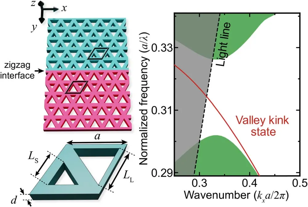
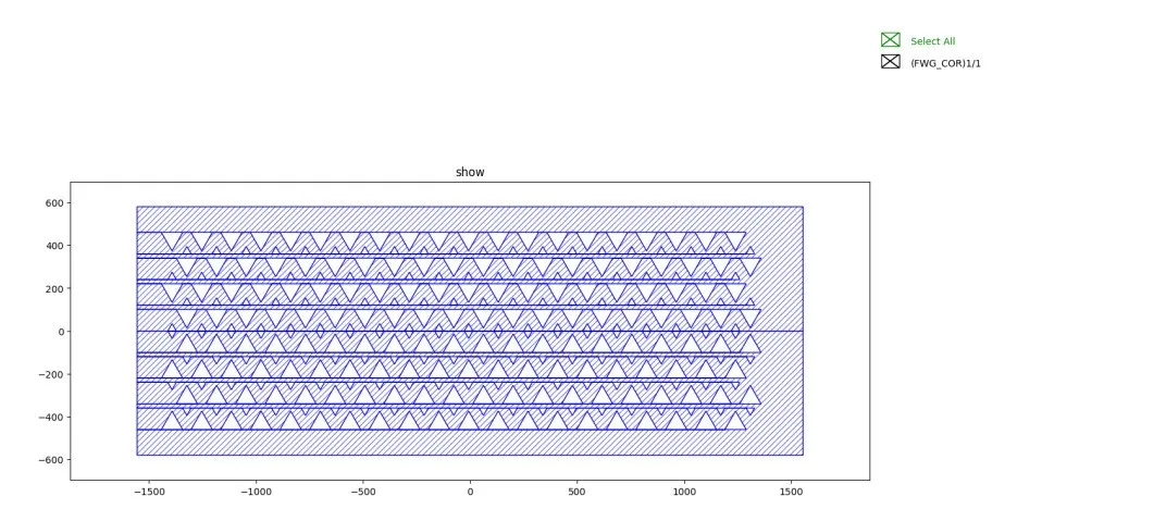
代码展示:
import math
from fnpcell import all as fp
from typing_extensions import Tuple, List, cast
from gpdk import all as pdk
from gpdk.technology import get_technology
from gpdk.technology.wg.types import CoreCladdingWaveguideType
import numpy as np


class PhC(fp.PCell):
    """
    Examples:
    PhC = PhC(PhC_row=6, PhC_column=12, PhC_rowgap=120, PhC_columngap=120, PhC_gap=200)
    """

    ## init parameters
    PhC_row: int = fp.PositiveIntParam(default=2)
    PhC_column: int = fp.PositiveIntParam(default=4)

    PhC_rowgap: float = fp.PositiveFloatParam(default=120)
    PhC_columngap: float = fp.PositiveFloatParam(default=120)
    PhC_gap: float = fp.FloatParam(default=20, min=0)

    wavegide_type: CoreCladdingWaveguideType = fp.WaveguideTypeParam(
        type=CoreCladdingWaveguideType, default=get_technology().WG.FWG.C.WIRE
    )

    def build(self):
        ## initial
        insts, elems, ports = super().build()

        ## define module
        ## double triangular
        para_gap = 80
        para_main = 50 * 2  # *np.sqrt(3)/2
        para_aux = 20 * 2  # *np.sqrt(3)/2
        PhC_gap = 0
        module_main = fp.el.Polygon(
            raw_shape=[
                (-para_main / 2, para_main * np.sqrt(3) / (4)),
                (para_main / 2, para_main * np.sqrt(3) / (4)),
                (0, -para_main * np.sqrt(3) / 2 + para_main * np.sqrt(3) / (4)),
            ],
            layer=self.wavegide_type.core_layer,
        )
        module_aux = fp.el.Polygon(
            raw_shape=[
                (-para_aux / 2, -para_aux * np.sqrt(3) / (4)),
                (para_aux / 2, -para_aux * np.sqrt(3) / (4)),
                (0, para_aux * np.sqrt(3) / 2 - para_aux * np.sqrt(3) / (4)),
            ],
            layer=self.wavegide_type.core_layer,
        )
        para_maingap = para_main * np.sqrt(3) / (4)
        para_auxgap = para_aux * np.sqrt(3) / (4)

        ## trans parameters
        PhC_width = (
            self.PhC_column * (np.sqrt(3) * para_gap)
            + para_main
            + 2 * self.PhC_columngap
        )
        PhC_height = (
            3 * para_gap * (self.PhC_row - 1)
            + 2 * para_gap
            + (para_maingap + para_auxgap)
            + self.PhC_rowgap
            + PhC_gap
        )

        ## design region
        design_rect = fp.el.Rect(
            width=PhC_width,
            height=PhC_height,
            layer=self.wavegide_type.core_layer,
            center=(0, PhC_height / 2),
        )

        for i in range(self.PhC_row):
            for j in range(self.PhC_column):
                x = (
                    -PhC_width / 2
                    + para_maingap
                    + self.PhC_columngap
                    + j * (para_gap * np.sqrt(3))
                )
                y = PhC_height - para_maingap - self.PhC_rowgap - i * (para_gap * 3)
                design_rect -= module_main.translated(x, y)
                design_rect -= module_aux.translated(
                    x + np.sqrt(3) / 2 * para_gap, y - 1 / 2 * para_gap
                )
                design_rect -= module_main.translated(
                    x + np.sqrt(3) / 2 * para_gap, y - 3 / 2 * para_gap
                )
                design_rect -= module_aux.translated(x, y - 2 * para_gap)
        elems += design_rect
        design_rect = design_rect | design_rect.v_mirrored()
        elems += design_rect
        return insts, elems, ports


if __name__ == "__main__":
    from gpdk.util.path import local_output_file

    gds_file = local_output_file(__file__).with_suffix(".gds")
    library = fp.Library()

    TECH = get_technology()
    # =============================================================

    library += PhC(PhC_column=20)

    # =============================================================
    fp.export_gds(library, file=gds_file)
    fp.plot(library)
3.2 A silicon-on-insulator slab for topological valley transport
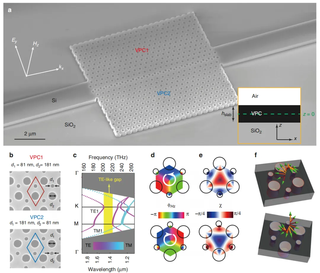
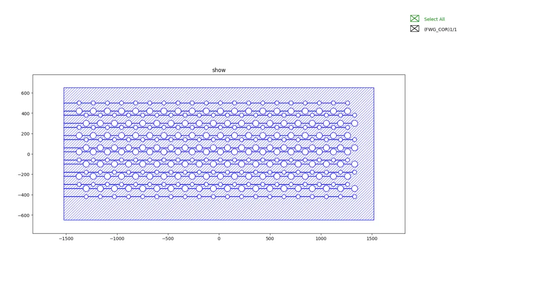
代码展示:
import math
from fnpcell import all as fp
from typing_extensions import Tuple, List, cast
from gpdk import all as pdk
from gpdk.technology import get_technology
from gpdk.technology.wg.types import CoreCladdingWaveguideType
import numpy as np


class PhC(fp.PCell):
    """
    Examples:
    PhC = PhC(PhC_row=6, PhC_column=12, PhC_rowgap=120, PhC_columngap=120, PhC_gap=200)
    """

    ## init parameters
    PhC_row: int = fp.PositiveIntParam(default=2)
    PhC_column: int = fp.PositiveIntParam(default=4)

    PhC_rowgap: float = fp.PositiveFloatParam(default=120)
    PhC_columngap: float = fp.PositiveFloatParam(default=120)
    PhC_gap: float = fp.FloatParam(default=20, min=0)

    wavegide_type: CoreCladdingWaveguideType = fp.WaveguideTypeParam(
        type=CoreCladdingWaveguideType, default=get_technology().WG.FWG.C.WIRE
    )

    def build(self):
        ## initial
        insts, elems, ports = super().build()

        ## define module
        ## double circle
        para_main = 30
        para_aux = 20
        para_gap = 80
        module_main = fp.el.Circle(
            radius=para_main,
            layer=self.wavegide_type.core_layer,
        )
        module_aux = fp.el.Circle(
            radius=para_aux,
            layer=self.wavegide_type.core_layer,
        )
        para_maingap = para_main
        para_auxgap = para_aux
        PhC_gap = para_gap

        ## trans parameters
        PhC_width = (
            self.PhC_column * (np.sqrt(3) * para_gap)
            + para_main
            + 2 * self.PhC_columngap
        )
        PhC_height = (
            3 * para_gap * (self.PhC_row - 1)
            + 2 * para_gap
            + (para_maingap + para_auxgap)
            + self.PhC_rowgap
            + PhC_gap
        )

        ## design region
        design_rect = fp.el.Rect(
            width=PhC_width,
            height=PhC_height,
            layer=self.wavegide_type.core_layer,
            center=(0, PhC_height / 2),
        )
        design_rect = design_rect | design_rect.v_mirrored()
        for i in range(self.PhC_row):
            for j in range(self.PhC_column):
                x = (
                    -PhC_width / 2
                    + para_maingap
                    + self.PhC_columngap
                    + j * (para_gap * np.sqrt(3))
                )
                y = PhC_height - para_maingap - self.PhC_rowgap - i * (para_gap * 3)
                design_rect -= module_aux.translated(x, y)
                design_rect -= module_main.translated(x, y - para_gap)
                design_rect -= module_aux.translated(
                    x + np.sqrt(3) / 2 * para_gap, y - 3 / 2 * para_gap
                )
                design_rect -= module_main.translated(
                    x + np.sqrt(3) / 2 * para_gap, y - 5 / 2 * para_gap
                )
        for i in range(self.PhC_row):
            for j in range(self.PhC_column):
                x = (
                    -PhC_width / 2
                    + para_maingap
                    + self.PhC_columngap
                    + j * (para_gap * np.sqrt(3))
                )
                y = (
                    PhC_height
                    - para_maingap
                    - self.PhC_rowgap
                    - (self.PhC_row + i) * (para_gap * 3)
                )
                design_rect -= module_main.translated(x, y)
                design_rect -= module_aux.translated(x, y - para_gap)
                design_rect -= module_main.translated(
                    x + np.sqrt(3) / 2 * para_gap, y - 3 / 2 * para_gap
                )
                design_rect -= module_aux.translated(
                    x + np.sqrt(3) / 2 * para_gap, y - 5 / 2 * para_gap
                )
        elems += design_rec

        return insts, elems, ports


if __name__ == "__main__":
    from gpdk.util.path import local_output_file

    gds_file = local_output_file(__file__).with_suffix(".gds")
    library = fp.Library()

    TECH = get_technology()
    # =============================================================

    library += PhC(PhC_column=20)

    # =============================================================
    fp.export_gds(library, file=gds_file)
fp.plot(library)需要注意的是,版图展示中的尺寸与论文并不一致,论文中的光子晶体参数设置与晶格常数息息相关。
4.参考文献
5.结论
本教程介绍了利用PhotoCAD工具完成任意光子晶体结构的实现,并通过两个案例展示了代码的可重复特性以及工具的易用性。
总部地址: 上海市郭守敬路 77 弄 3 幢 402 室
电话: 028-81756623
@2021 - 2025 Whoscored中文官网 Latitude Design Automation Inc.
粤ICP备2021098982号-1 | 粤公网安备 44030502008170号
 微信公众号
 bilibili
 微信视频号